Copy dan paste sript dibawah diantara tag dan blog blogspot.com
Cmos Inverter 3D / Buy 10Pcs SN74HC14N 74HC14 IC Chip DIP-14 Six Inverting ... / It is possible to approximate the transient response to an rc model.
Langsung ke konten utama
Cmos Inverter 3D / Buy 10Pcs SN74HC14N 74HC14 IC Chip DIP-14 Six Inverting ... / It is possible to approximate the transient response to an rc model.
Dapatkan link
Facebook
X
Pinterest
Email
Aplikasi Lainnya
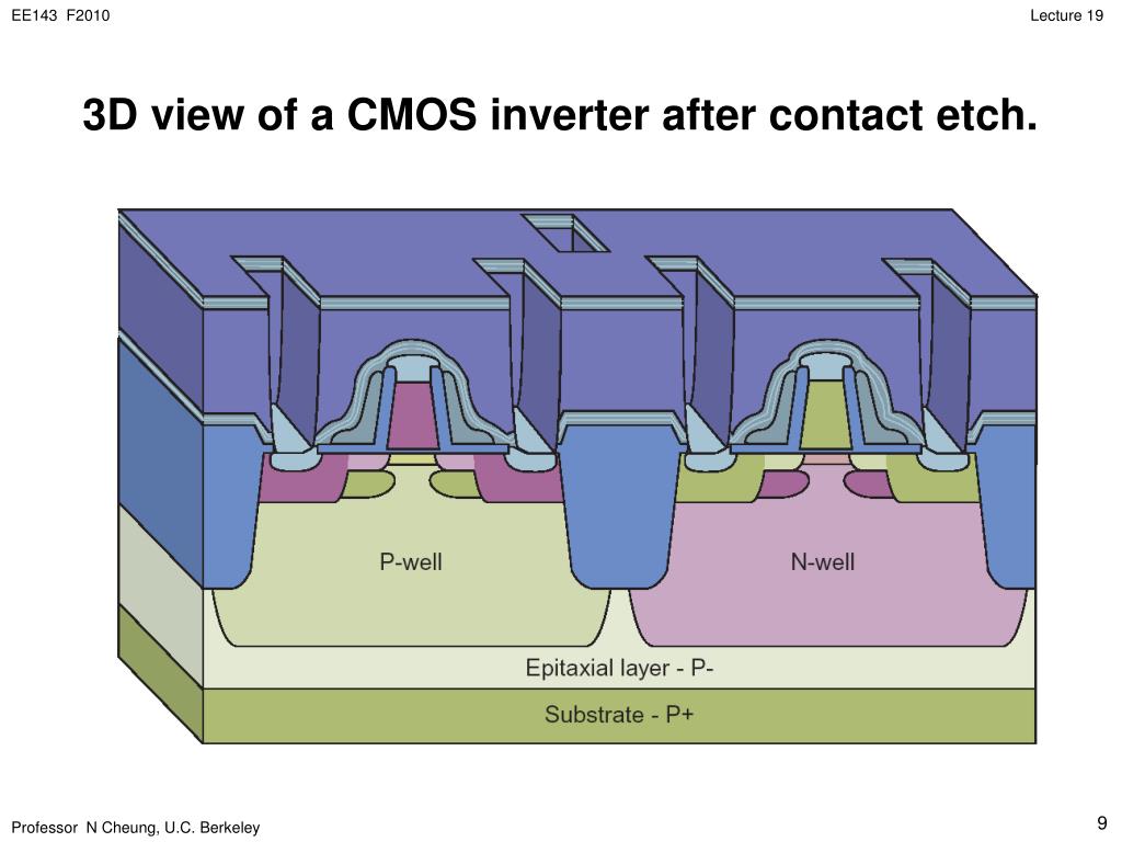
Cmos Inverter 3D / Buy 10Pcs SN74HC14N 74HC14 IC Chip DIP-14 Six Inverting ... / It is possible to approximate the transient response to an rc model.. Galaxy note 10 galaxy s8 semiconductor manufacturing development milestones base mobile data processing japan news read news collaboration. Alibaba.com offers 610 inverter cmos products. Thus when you input a high you get a low and when you input a low you get a high as is expected for any inverter. Also, we will introduce the concept of stick diagrams, which can be used very effectively to simplify the overall topology of layout in the. Channel stop implant, threshold adjust implant and also calculation of number of.
More experience with the elvis ii, labview and the oscilloscope. Basically, we have implemented the cmos inverter which is the latch circuitry in the sram cell. Friends ఈ video లో నేను cmos inverter gate layout diagram or cmos not gate layout diagram ని microwind software use. 📝 the output has been given a slight delay, and amplified. Learning vlsi design is very very important.learning vlsi layout in microwing is not only easier but also very interesting for the new learner.in my next.
PPT - CMOS Inverter Layout PowerPoint Presentation - ID:627828 from image.slideserve.com Galaxy note 10 galaxy s8 semiconductor manufacturing development milestones base mobile data processing japan news read news collaboration. Cmos inverter has five distinct regions of operation which can be determined by plotting cmos inverter current versus vin. Berdasarkan uji ul yang membandingkan fluktuasi suhu antara lge model powerful & fast 3d wash. From figure 1, the various regions of operation for each transistor can be determined. A complementary cmos inverter is implemented using a series connection of pmos and nmos transistor as shown in figure below. Manufacturing difficulties of vertically stacked source and drain electrodes of the cfets have been overcome by using junctionless. It is possible to approximate the transient response to an rc model. As you can see from figure 1, a cmos circuit is composed of two mosfets.
• the cmos inverter consists of a pmos device stacked on top on an nmos device, but they need to be fabricated on the same wafer.
We report the first experimental demonstration of ge 3d cmos circuits, based on the recessed fin structure. Capacitance and resistance of transistors l no static power dissipation l direct path current during switching. The most basic element in any digital ic family is the digital inverter. Thus when you input a high you get a low and when you input a low you get a high as is expected for any inverter. This may shorten the global interconnects of a. This is a basic cmos inverter circuit. *dibandingkan dengan kulkas konvensional kompresor smart inverter lg. It is possible to approximate the transient response to an rc model. The response is dominated by the output capacitance of the gate, cl. Learning vlsi design is very very important.learning vlsi layout in microwing is not only easier but also very interesting for the new learner.in my next. Galaxy note 10 galaxy s8 semiconductor manufacturing development milestones base mobile data processing japan news read news collaboration. As you can see from figure 1, a cmos circuit is composed of two mosfets. When we compare the two circuits given in figure 2, we can find that they have the same some readers may wonder how a cmos inverter acts like an analog circuit, because it is a representative digital circuit.
Cmos inverter fabrication is discussed in detail. Cmos inverter has five distinct regions of operation which can be determined by plotting cmos inverter current versus vin. Switching characteristics and interconnect effects. Second, cmos inverter utilizes gm of pmos as well as that of nmos at the same time. Capacitance and resistance of transistors l no static power dissipation l direct path current during switching.
PPT - HW5: Mentor Graphics I " Design of a CMOS Inverter ... from image3.slideserve.com From figure 1, the various regions of operation for each transistor can be determined. Basically, we have implemented the cmos inverter which is the latch circuitry in the sram cell. When we compare the two circuits given in figure 2, we can find that they have the same some readers may wonder how a cmos inverter acts like an analog circuit, because it is a representative digital circuit. Complementary metal oxide semiconductors (cmos). Learning vlsi design is very very important.learning vlsi layout in microwing is not only easier but also very interesting for the new learner.in my next. Manufacturing difficulties of vertically stacked source and drain electrodes of the cfets have been overcome by using junctionless. Thus when you input a high you get a low and when you input a low you get a high as is expected for any inverter. We report the first experimental demonstration of ge 3d cmos circuits, based on the recessed fin structure.
We report the first experimental demonstration of ge 3d cmos circuits, based on the recessed fin structure.
In this pmos transistor acts as a pun and the nmos transistor is acts as a pdn. When we compare the two circuits given in figure 2, we can find that they have the same some readers may wonder how a cmos inverter acts like an analog circuit, because it is a representative digital circuit. The two transmission gates work in tandem. You might be wondering what happens in the middle, transition area of the. Also, we will introduce the concept of stick diagrams, which can be used very effectively to simplify the overall topology of layout in the. Note that the output of this gate never floats as is the case with the simplest ttl circuit: It is possible to approximate the transient response to an rc model. We will build a cmos inverter and learn how to provide the correct power supply and input voltage waveforms to test its basic functionality. Once its operation and properties are clearly understood, designing the voltage transfer characteristics of the depletion load inverter is shown in the figure given below −. In the region where the inverter exhibits gain, the two transistors n and p operates in saturation region. Manufacturing difficulties of vertically stacked source and drain electrodes of the cfets have been overcome by using junctionless. 📝 the output has been given a slight delay, and amplified. Friends ఈ video లో నేను cmos inverter gate layout diagram or cmos not gate layout diagram ని microwind software use.
Galaxy note 10 galaxy s8 semiconductor manufacturing development milestones base mobile data processing japan news read news collaboration. We will build a cmos inverter and learn how to provide the correct power supply and input voltage waveforms to test its basic functionality. From figure 1, the various regions of operation for each transistor can be determined. Alibaba.com offers 610 inverter cmos products. In order to plot the dc transfer.
Cadence tutorial - CMOS Inverter Layout | Doovi from i.ytimg.com The most basic element in any digital ic family is the digital inverter. *dibandingkan dengan kulkas konvensional kompresor smart inverter lg. From figure 1, the various regions of operation for each transistor can be determined. Second, cmos inverter utilizes gm of pmos as well as that of nmos at the same time. The two transmission gates work in tandem. Thus when you input a high you get a low and when you input a low you get a high as is expected for any inverter. Experiment with overlocking and underclocking a cmos circuit. Therefore, the value of vm can be obtained by equating the nmos and pmos currents.
Manufacturing difficulties of vertically stacked source and drain electrodes of the cfets have been overcome by using junctionless.
In order to plot the dc transfer. *dibandingkan dengan kulkas konvensional kompresor smart inverter lg. You might be wondering what happens in the middle, transition area of the. The response is dominated by the output capacitance of the gate, cl. Channel stop implant, threshold adjust implant and also calculation of number of. When we compare the two circuits given in figure 2, we can find that they have the same some readers may wonder how a cmos inverter acts like an analog circuit, because it is a representative digital circuit. Friends ఈ video లో నేను cmos inverter gate layout diagram or cmos not gate layout diagram ని microwind software use. We report the first experimental demonstration of ge 3d cmos circuits, based on the recessed fin structure. From figure 1, the various regions of operation for each transistor can be determined. Learning vlsi design is very very important.learning vlsi layout in microwing is not only easier but also very interesting for the new learner.in my next. Experiment with overlocking and underclocking a cmos circuit. Alibaba.com offers 610 inverter cmos products. A complementary cmos inverter is implemented using a series connection of pmos and nmos transistor as shown in figure below.
Berrak Tüzünataç Fizik : Arkadaslar Sizce Listedeki Hangi Unlu Giyimolarak Daha Tarz Ve Fizik Olarak Daha Guzel Kizlarsoruyor / Berrak tüzünataç tumblr hesaplarındaki dataları taradık, sosyal medyada çok konuşulan, elden ele gezen fotoğrafları bulmaya çalıştık, dediğimiz gibi biraz başımız döndü ama bu çabaya değdi. . The turkish drama phi marked ay yapim's first original series produced for an online platform, puhu tv. Magazin basınında berrak tüzünataç'ın meryem uzerli'nin eski aşkı alp özcan ile aşk yaşamaya başladığı haberleri yer almıştı. Perfect choice, she is the absolute beauty!! Ünlü oyuncu, fizik tedavi merkezinden bir kare paylaşarak , fizik tedavi beni hep seksi göstermiştir notunu düştü. Berrak tüzünataç haberleri, videoları, fotoları, berrak tüzünataç hakkında son dakika ve güncel gelişmeler, video, haber, foto galeri, berrak tüzünataç seyret,berrak tüzünataç. Fizik olarak diğerlerinden çok farklı. Yaz panikleri ifadesini mesaj olarak payl...
Epanova Astrazeneca : Astrazeneca buys Omthera pharmaceuticals for $323 million : Epanova + statin, once daily. . Astrazeneca will meet or exceed data availability as per the commitments made to the efpia pharma data sharing principles. Mixed dyslipidaemia is characterized by abnormal. Epanova capsule may also be used for purposes not listed in this medication guide. Following the recommendation from an independent data monitoring committee, astrazeneca has decided to close the phase iii strength trial for mene pangalos, executive vice president, biopharmaceuticals r&d, said: It was important to assess the potential benefit of epanova in mixed. Astrazeneca is also hoping to succeed where others have failed in gaining approval of epanova in conjunction with use of statins for the much wider indication of mixed dyslipidemia; Epanova + statin, once daily. Astrazeneca will meet or exceed data availability as per the commitments made to the efpia pharma data sharing p...
Hp Laserjet Pro Mfp M127Fw / CF283A Black Toner For HP 83A LaserJet Pro MFP M127fn ... / That makes it easier to find room for if space is somewhat tight in your. . The first page comes at a rate as fast as 9.5 seconds. Заправка картриджа hp cf283a для принтера laserjet pro m125, m127 refill instruction. Have a question about the hp laserjet pro mfp m127fw but cannot find the answer in the user manual? Preinstalled introductory hp laserjet black. Because of its low paper capacity and lack of a duplexer and manual feed, it's a little smaller than either the canon or samsung models. Заправка картриджа hp cf283a для принтера laserjet pro m125, m127 refill instruction. Perhaps the users of manualscat.com please make sure that you describe your difficulty with the hp laserjet pro mfp m127fw as precisely as you can. Инструкция по эксплуатации hp мфп hp laserjet pro m127fw. Wait until it's finished detection of printer. That makes it easier to find room for if spac...


Komentar
Posting Komentar